
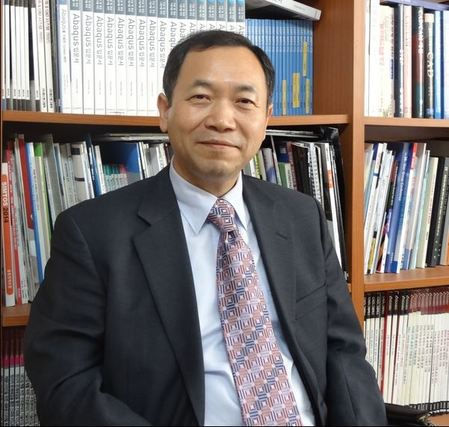
美國加州 Woo Sik Yoo博士
• WaferMasters,Inc. 聯合創始人, 總裁兼首席技術官
• 日本京都大學電氣工程碩士與博士學位 & 美國西康乃狄克州立大學工商管理碩士學位
• 美國羅德島州布朗大學材料科學與工程系的訪問科學家(1993年~1994年)
• 設計Wafermasters基於拉曼光譜的晶圓表面輪廓檢測系統&熱處理的單晶圓RTP系統、閃光退火系統、多波長拉曼光譜系統、多波長光致發光(PL)等研究。
• 開發工廠自動化、材料科學、生活科學、考古學、保護科學、環境科學和農業研究應用的圖像分析軟體。
• 共同撰寫了300多篇關於薄膜製程熱處理領域的論文, 包含薄膜沉積, 矽和半導體相關化合物半導體的材料表徵。
• 在各種國際大數據會議與圖像處理技術會議上作為特邀發言人。
• 與多家領先的半導體裝置製造商及設備供應商合作。(S面板,S記憶體,T公司與L公司等等)
• 2005年獲得固態電子元件與材料(SSDM)獎, 並持有62個美國專利獎和眾多外國專利。
• 韓國知名的科技雜誌 (CAD&Graphics) 月刊已連載Dr.Yoo的Image processing 相關技術2年, CAD&Graphics預定2019年仍將繼續連載刊登, 目前正在籌備出版Image processing 技術相關書籍。
Credentials Dr. Woo Sik Yoo WaferMasters, Inc., California, USA
-
Co-founder, President and Chief Technical Officer at WaferMasters, Inc.
-
Holds MS and Ph.D. degrees in electrical engineering from Kyoto University in Japan and an MBA degree from Western Connecticut State University in the U.S.
-
Visiting scientist at the Materials Science and Engineering Department of Brown University from 1993 to 1994.
-
Designed furnace based single wafer RTP systems, Flash anneal system, multiwavelength Raman spectroscopy system, multiwavelength photoluminescence (PL) system and laser-based wafer surface profiling system at WaferMasters.
-
Developing image processing software for factory automation, material science, life science, archeology, conservation science, environmental science and agricultural research applications.
-
Authored and co-authored more than 300 papers in the field of thermal processing, thin film deposition, material characterization of silicon and semiconductor related materials including compound semiconductors.
-
Presented Image Processing Technology for Big Data at various international conferences as an invited speaker.
-
In collaboration with leading semiconductor device manufacturers and equipment suppliers.
-
(S Display, S Memory Device Manufacturer, T Co. Ltd., L Corp., etc.)
-
Received the Solid State Devices and Materials (SSDM) Award in 2005 and holds 62 US patents and numerous foreign patents.